PRE / 01OEM / ODM review
Laser metal deposition cladding system
Deposit metal onto a substrate using a specified laser-cladding or directed-energy-deposition route.
Key decisions
View specifications↗Powder, substrate and dilution acceptance.

IndustryApex · Engineering-led equipment supply
Find the equipment, interfaces and acceptance criteria for your next production project. Start with the result you need.

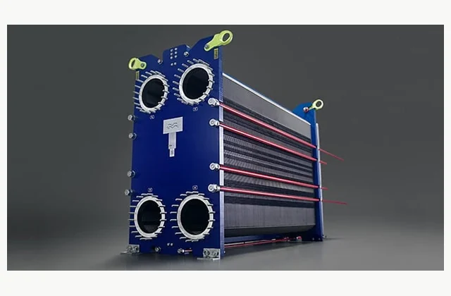
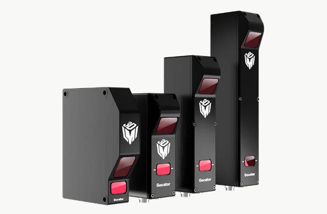
Related equipment references. The complete configuration is confirmed for your project.
Choose your application
The system library
Try a broader equipment or process term, or describe the application to our team.
Ask for an engineering review ↗05 / 194 system families
Specify the material, feature and surface result.
Deposit metal onto a substrate using a specified laser-cladding or directed-energy-deposition route.
Powder, substrate and dilution acceptance.
Machine small features with an ultrashort-pulse laser process selected for the material.
Feature geometry, material response and debris.
Create controlled surface texture using a laser process.
Texture geometry, depth and surface function.
Join compatible material interfaces through an engineered vacuum diffusion-bonding process.
Interface preparation, pressure and thermal cycle.
Consolidate suitable powders using a spark-plasma-sintering process.
Powder properties, tooling and consolidation cycle.
Deposit a specified thin-film coating using magnetron sputtering.
Substrate, coating stack and vacuum boundary.
Deposit specified films using plasma-enhanced chemical vapor deposition.
Precursors, film specification and exhaust treatment.
Deposit controlled thin films by atomic-layer-deposition cycles suited to the substrate and chemistry.
Substrate geometry, film thickness and precursor handling.
Apply a functional coating to a moving web using an integrated coating and curing line.
Web tension, coating uniformity and curing.
Meter a specified liquid coating through a slot die onto a suitable substrate.
Rheology, coat weight and substrate flatness.
Apply thin liquid coatings using an ultrasonic spray system.
Droplet distribution, coverage and drying.
Condition surfaces or edges by moving an abrasive medium through specified flow paths.
Internal passage, medium and edge condition.
Machine conductive material features using a micro-scale electrical-discharge process.
Electrode geometry, dielectric and feature tolerance.
Produce metal powder through an atomization system qualified for the alloy and required powder properties.
Alloy, particle distribution and powder containment.
Machine suitable optical or precision surfaces using a thermally controlled diamond-turning system.
Material machinability, surface form and thermal stability.
Correct a measured optical surface using a calibrated ion-beam removal process.
Surface error map, removal function and final metrology.
Compact suitably packaged powder bodies using approximately uniform external fluid pressure at a cold processing stage.
Powder preparation, flexible tooling and green-part requirements.
Remelt a suitable consumable electrode under vacuum to develop an ingot with a defined metallurgical quality objective.
Electrode quality, alloy refining objective and ingot acceptance.
Melt and refine suitable reactive or refractory feedstocks using an electron beam and a defined cold-hearth process route.
Alloy feed, refining objective and vacuum melting boundary.
Introduce a controlled near-surface compressive residual-stress treatment using laser-generated shock loading on suitable components.
Material response, treatment access and residual-stress evidence.
Form an oxide-based surface layer on suitable light-alloy parts using a controlled plasma electrolytic oxidation process.
Substrate alloy, coating properties and electrolyte management.
Deposit a selected thermal-spray coating using a high-velocity oxygen-fuel spray process and an engineered handling cell.
Powder chemistry, substrate preparation and coating acceptance.
Correct suitable optical surfaces through controlled magnetorheological polishing with a measured removal function.
Optical material, removal function and final surface metrology.
Deposit a defined thin metal layer onto a flexible moving substrate within a roll-to-roll vacuum coating installation.
Web behavior, deposited film and vacuum process conditions.
Grow a qualified silicon-carbide crystal using a physical-vapor-transport process.
Source material, seed, boule objective, thermal design, vacuum and gas utilities.
Grow specified silicon crystals through a qualified melt-pulling process.
Feedstock, crystal geometry, dopant objective, crucible, atmosphere and thermal requirements.
Grow and refine suitable silicon rods using an engineered floating molten zone.
Feed-rod quality, crystal diameter, doping, induction design and atmosphere boundary.
Grow a specified sapphire crystal through an agreed qualified thermal route.
Growth method, charge purity, crystal geometry, thermal design and atmosphere utilities.
Deposit qualified gallium-nitride epitaxial layers on specified semiconductor substrates.
Substrate, layer objectives, uniformity, precursor interfaces, abatement and analytical requirements.
Grow specified thin-film structures through an engineered molecular-beam epitaxy process.
Materials, substrate, source configuration, layer sequence, vacuum and in-situ diagnostics.
Grow qualified diamond material using an engineered chemical-vapor deposition route.
Substrate format, material objective, gas interfaces, thermal control and analytical acceptance.
Grow specified compound-semiconductor layers through a qualified hydride-vapor-phase process.
Material system, substrate, growth objective, gas compatibility, abatement and metrology.
Planarize specified wafer materials using a qualified combined chemical and mechanical process.
Wafer size, film stack, removal target, defect limits, slurry and cleaning interfaces.
Thin suitable wafers through an engineered supported grinding and stress-management workflow.
Wafer material, final thickness, temporary support, device features and downstream singulation.
Singulate qualified wafers using an engineered internal laser-modification and separation process.
Wafer transparency, device layout, thickness, street geometry, tape and separation method.
Join specified wafer structures with qualified alignment and bonding conditions.
Wafer materials, size, bond method, alignment, surface condition and contamination limits.
Apply a qualified localized thermal treatment to specified semiconductor structures.
Wafer stack, treatment objective, optical response, thermal budget and process uniformity.
Introduce specified dopant species into suitable substrates through a qualified ion-beam process.
Substrate, dopant, dose and energy objectives, throughput, handling and abatement interfaces.
Pattern specified materials through an engineered inductively coupled plasma etch process.
Material stack, mask, profile target, selectivity, substrate cooling and exhaust treatment.
Form qualified deep structures in suitable substrates through an engineered plasma etch sequence.
Substrate, mask, feature geometry, depth, sidewall targets and thermal control.
Clean or etch specified semiconductor materials in a qualified chemical-processing installation.
Substrates, chemistry compatibility, bath sequence, particle limits, handling and exhaust interfaces.
Release specified microstructures through a qualified vapor-phase sacrificial-material removal process.
Device stack, sacrificial material, structural materials, release geometry and exhaust treatment.
Apply a qualified short-duration thermal cycle to specified wafers.
Wafer materials, thermal budget, atmosphere, temperature measurement and device-stack requirements.
Process specified wafers through a qualified thermal oxidation or diffusion sequence.
Wafer size, process atmosphere, layer or dopant objective, contamination limits and batch format.
Write specified resist patterns using an engineered electron-beam lithography workflow.
Pattern dimensions, substrate, resist, alignment, write field and charging behavior.
Align and expose specified resist-coated substrates through a qualified optical mask process.
Substrate, mask, resist, alignment accuracy, exposure mode and required feature geometry.
Replicate specified micro- or nanoscale patterns through a qualified imprint process.
Template, substrate, resist, feature dimensions, residual layer and defect criteria.
Image specified PCB resist patterns using a qualified direct optical exposure process.
Panel dimensions, resist response, feature geometry, registration and handling requirements.
Prepare and develop specified wafer resists through an engineered coating and processing sequence.
Wafer format, resist chemistry, film target, baking, developing and transfer interfaces.
Remove qualified resist or organic residues from specified substrates using a controlled plasma process.
Resist, substrate stack, residue, thermal limits, endpoint method and exhaust requirements.
Deposit specified thin-film materials through qualified electron-beam evaporation.
Source materials, substrate geometry, thickness, temperature budget and coating uniformity.
Deposit suitable materials through an engineered thermal evaporation process.
Evaporant, substrate, thermal budget, thickness, uniformity and vacuum requirements.
Form specified films through a qualified ion-beam-driven deposition process.
Film material, optical or mechanical objective, substrate, thickness and contamination limits.
Deposit qualified protective films using an engineered cathodic-arc process.
Substrate alloy, coating chemistry, part geometry, temperature budget and finish requirements.
Apply a specified thermal-spray coating through an engineered air-fuel spray installation.
Feedstock, substrate, coating function, access geometry, finishing and utility requirements.
Build or restore qualified metal features through an engineered cold-spray deposition process.
Powder properties, substrate, build geometry, bonding objective and post-processing.
Deposit specified coatings using an engineered plasma process with liquid-suspension feedstock.
Suspension stability, coating chemistry, substrate, morphology target and exhaust requirements.
Harden selected suitable metal surfaces through a qualified localized laser thermal cycle.
Alloy, initial structure, target case, geometry, surface condition and distortion limits.
Treat suitable metal surfaces through a qualified plasma nitriding process.
Alloy, surface preparation, case objective, masking, geometry and temperature limits.
Form a qualified boride surface layer on suitable materials through an engineered thermal process.
Alloy, desired layer, geometry, dimensional allowance and service or inspection requirements.
Carburize and process suitable steel parts through a qualified low-pressure thermal route.
Steel grade, case target, geometry, loading, distortion limits and quench method.
Apply a qualified isothermal transformation route to suitable metal components.
Material, section thickness, target microstructure, transfer limits and cleaning requirements.
Refine suitable consumable electrodes through an engineered electroslag remelting process.
Alloy, electrode condition, ingot geometry, inclusion objective, slag compatibility and utilities.
Cast qualified alloy components with a specified directional-solidification objective.
Alloy, mold and core, grain objective, part geometry, thermal design and inspection plan.
Fill suitable molds using an engineered vacuum and pressure-assisted casting sequence.
Alloy, mold geometry, fill objective, atmosphere, thermal conditions and finishing requirements.
Melt qualified alloys under an engineered vacuum or controlled-atmosphere induction process.
Alloy, charge form, batch mass, atmosphere, crucible compatibility and casting interface.
Cast a specified copper feed into rod through an engineered upward continuous-casting process.
Copper chemistry, rod dimensions, withdrawal duty, cooling and downstream drawing requirements.
Produce a specified metal strip through an engineered twin-roll solidification process.
Alloy, melt quality, strip width and gauge, surface target and cooling system.
Build qualified metal preforms through an engineered atomization and deposition process.
Alloy, melt quality, preform geometry, atomization conditions and downstream consolidation.
Form qualified green metal parts by binder jetting followed by a defined debinding and sintering route.
Powder, binder, geometry, green handling, sintering supports and final-property requirements.
Build qualified metal parts using electron-beam powder-bed fusion.
Alloy powder, geometry, support strategy, vacuum, post-processing and inspection objectives.
Build qualified metal shapes through controlled arc deposition of wire feedstock.
Alloy wire, geometry, deposition path, interpass limits, machining allowance and inspection plan.
Create qualified metal parts through feedstock extrusion, debinding and sintering.
Feedstock, geometry, supports, debinding compatibility, furnace route and final properties.
Print qualified ceramic green parts using a photosensitive slurry and defined thermal post-processing.
Ceramic, slurry stability, feature geometry, support design, debinding and sintering requirements.
Deposit qualified ceramic pastes in controlled paths before an agreed drying and sintering sequence.
Paste, nozzle, geometry, drying behavior, supports and final material requirements.
Produce qualified ceramic parts through feedstock molding, debinding and sintering.
Ceramic powder, binder, geometry, tooling, debinding route and final tolerances.
Densify suitable ceramic bodies under a qualified combination of heat and uniaxial pressure.
Powder, die material, geometry, atmosphere, pressure direction and property objectives.
Process suitable ceramic materials using a qualified microwave-assisted thermal route.
Ceramic dielectric behavior, geometry, loading, thermal objective and atmosphere.
Densify qualified silicon-carbide bodies through an engineered pressureless sintering route.
Powder and additives, green geometry, atmosphere, shrinkage allowance and property targets.
Form qualified reaction-bonded silicon-carbide components through an engineered infiltration process.
Preform composition, pore network, geometry, infiltrant, material limits and inspection requirements.
Densify specified porous preforms through a qualified chemical-vapor-infiltration process.
Preform architecture, chemistry, pore access, density target, gas distribution and abatement.
Densify qualified composite preforms through an agreed polymer-infiltration and pyrolysis route.
Preform, precursor compatibility, infiltration method, thermal cycle and property targets.
Cure qualified composite assemblies within a controlled pressure and thermal installation.
Resin system, layup, part and tool envelope, cure profile, vacuum and instrumentation.
Inject qualified resin into a prepared reinforcement and closed mold within an engineered RTM process.
Reinforcement, resin rheology, mold geometry, injection boundary and final laminate properties.
Produce specified reinforcement preforms through an engineered braiding process.
Fiber format, preform geometry, braid architecture, tension, handling and downstream molding.
Place qualified reinforcement tows along engineered paths on a defined composite tool.
Tow format, material tack or thermal behavior, tool geometry, paths and defect criteria.
Lay qualified composite tape onto a specified tool or flat charge through an engineered process.
Tape material, width, tool geometry, layup sequence, compaction and cure interfaces.
Consolidate qualified thermoplastic laminates through an engineered heat and pressure sequence.
Matrix and reinforcement, layup, tooling, temperature uniformity, cooling and dimensional targets.
Form specified three-dimensional reinforcement architectures through a qualified weaving process.
Fiber materials, three-dimensional architecture, preform envelope, tension and downstream consolidation.
Form qualified fine-fiber webs from suitable solutions or melts through an engineered electrospinning process.
Polymer, feed properties, solvent management, fiber target, collector and web-handling requirements.
Produce qualified fibers through an engineered centrifugal spinning and collection process.
Feed rheology, temperature or solvent boundary, fiber target, collector and throughput objective.
Create specified periodic surface patterns through a qualified optical-interference process.
Material, pattern period, depth, area, surface finish and alignment requirements.
Build specified metal microstructures through a qualified electroforming and release process.
Metal chemistry, master geometry, thickness, stress limits, release and inspection methods.
Build qualified metal laminates through controlled ultrasonic joining of successive layers.
Foil material, layer geometry, interface cleanliness, embedded features and post-machining.
Place and attach individual dies to a defined package substrate.
Die dimensions, adhesive, substrate, placement tolerance and curing route.
Connect package pads using controlled ultrasonic wire bonding.
Wire material, diameter, pad metallurgy, loop geometry and heating.
Join bumped dies using controlled alignment pressure and heat.
Bump pitch, coplanarity, bonding force, thermal profile and substrate warpage.
Embed placed dies into a reconstructed wafer for subsequent processing.
Die layout, carrier, molding compound, shrinkage and release process.
Encapsulate a defined semiconductor package using a compression mold process.
Package cavity, molding compound, pressure, thermal profile and vacuum.
Fill defined chip-substrate gaps with a controlled encapsulant.
Gap geometry, material rheology, dispense path, heating and cure.
Prepare package surfaces using a qualified plasma cleaning recipe.
Surface materials, contamination, plasma gas, power and exposure.
Separate molded packages along a defined saw street layout.
Panel geometry, street width, blade, coolant and package support.
Place solder spheres onto patterned package pads before reflow.
Ball diameter, pitch, flux, substrate flatness and missing-ball detection.
Attach a package lid using an agreed adhesive solder or sealing route.
Lid geometry, seal material, atmosphere, thermal limits and fixture.
Create microvias in a specified circuit-board material stack.
Dielectric, copper thickness, via diameter, registration and residue control.
Prepare drilled interconnect surfaces for metallization.
Resin system, smear, hole aspect ratio, chemical stages and rinse controls.
Deposit an initial conductive copper layer on qualified hole surfaces.
Substrate, activation, bath chemistry, loading and process controls.
Plate copper into selected interconnect geometries using controlled chemistry.
Via geometry, current waveform, agitation, additive control and thickness.
Apply and pattern a protective mask over a defined PCB surface.
Mask chemistry, coating thickness, registration, exposure and cure.
Fill specified PCB holes with resin under controlled pressure and vacuum.
Hole geometry, resin viscosity, fixture, fill sequence and cure.
Separate finished board outlines using a qualified laser cutting path.
Board stack, outline, sensitive parts, cutting parameters and extraction.
Transport panels through a controlled continuous metal plating process.
Panel dimensions, chemistry, current density, agitation and dwell time.
Apply a specified solderable protective finish to exposed conductive features.
Chosen finish chemistry, pad metallurgy, thickness and compatibility.
Prepare polished circuit-board cross-sections for interconnect analysis.
Coupon location, mounting, cutting, grinding, polishing and edge retention.
Generate a specified optical surface before precision polishing.
Glass, blank geometry, curvature, tool path, coolant and stock allowance.
Correct a defined aspheric surface using a controlled polishing process.
Surface prescription, aperture, material, removal model and metrology feedback.
Machine lens edges relative to a defined optical axis.
Lens shape, edge geometry, centration reference, clamping and coating.
Replicate optical surfaces by controlled molding of qualified glass preforms.
Glass transition behavior, mold material, atmosphere, force and thermal cycle.
Polish optical surfaces using matched pitch tooling and abrasive slurry.
Optic material, curvature, lap compliance, slurry and conditioning.
Apply localized removal through a compliant rotating polishing tool.
Surface slope, aperture, bonnet pressure, tool influence and metrology.
Shape glass over a defined mold using a controlled thermal cycle.
Glass composition, thickness, mold geometry, support and temperature profile.
Apply light-absorbing material to specified lens or optical assembly edges.
Edge geometry, coating rheology, masking, adhesion and curing.
Align and cement optical elements within a defined bonded group.
Optic geometry, cement, wedge, centration, curing and handling.
Deposit a defined optical multilayer using ion-assisted evaporation control.
Optical stack, substrate, source materials, ion conditions and monitoring.
Deposit controlled glass layers inside a rotating silica tube.
Glass dopants, gas delivery, burner traverse, tube geometry and collapse.
Build glass soot on a rotating target before consolidation.
Precursor chemistry, burner configuration, soot density and deposition schedule.
Grow a glass soot preform axially using controlled vapor deposition.
Gas chemistry, burner positions, growth rate and thermal conditions.
Deposit internal optical glass layers using a traveling plasma zone.
Tube material, dopants, plasma power, pressure and traverse.
Densify deposited silica soot under a defined gas and heat schedule.
Soot chemistry, geometry, dehydration gases, temperature and atmosphere.
Draw a specified preform into a dimensionally controlled optical fiber.
Preform, furnace, draw tension, diameter feedback and coating interfaces.
Apply and cure protective polymer layers on moving fiber.
Fiber speed, coating geometry, resin, concentricity and curing dose.
Apply controlled tensile proof loading while transferring optical fiber.
Fiber type, proof load, contact geometry, speed and break detection.
Arrange and bond defined fiber groups into a controlled ribbon geometry.
Fiber count, pitch, matrix resin, cure and fiber identification.
Write a defined refractive-index pattern using a qualified optical exposure process.
Fiber photosensitivity, grating period, laser exposure, tension and thermal state.
Produce controlled green ceramic sheets from a defined slurry.
Powder, binder, solvent, viscosity, casting gap and drying profile.
Print conductive or functional patterns onto unfired ceramic tapes.
Paste rheology, screen geometry, registration and green-sheet stability.
Align and consolidate printed ceramic layers before firing.
Layer count, fiducials, pressure, temperature and release films.
Cut unfired ceramic laminates into specified component geometries.
Laminate thickness, pattern location, blade geometry and support.
Remove organics from green ceramics using a controlled atmosphere profile.
Binder chemistry, loading, gas flow, heating rate and exhaust.
Cofire ceramic and electrode layers within a specified redox environment.
Ceramic chemistry, electrode metal, oxygen activity and thermal profile.
Apply conductive termination material to defined component ends.
Component dimensions, paste, immersion depth, drying and orientation.
Plate an agreed finish onto metallized ceramic component terminations.
Base metal, finish stack, bath chemistry, barrel loading and current.
Adjust printed resistor values using controlled laser material removal.
Resistor material, target value, trim geometry, pulse settings and measurement.
Align domains in specified piezoelectric components under controlled field and heat.
Ceramic composition, geometry, electrodes, field, temperature and dwell.
Stabilize precursor fibers through controlled oxidative heating and tension.
Precursor chemistry, tow size, oxygen, temperatures, residence and tension.
Convert stabilized fibers into carbon-rich fibers under inert conditions.
Precursor state, tow path, atmosphere, tension and heating profile.
Heat treat carbon fibers to a defined structural state.
Fiber type, thermal profile, tension, atmosphere and electrical heating.
Condition fiber surfaces and apply protective sizing before winding.
Fiber chemistry, treatment method, sizing, pickup and drying conditions.
Remove specified graphite impurities through a defined thermal purification route.
Graphite form, impurity assay, atmosphere, temperature and exhaust handling.
Carbonize an applied organic coating on qualified graphite anode particles.
Coating precursor, graphite, residence, atmosphere, heating and particle transport.
Grow a specified graphene layer using catalytic vapor deposition.
Catalyst substrate, precursor, gas purity, pressure and thermal program.
Produce a defined dispersed graphene fraction from layered feedstock.
Feed graphite, solvent, energy input, separation and product specification.
Grow nanotubes from a qualified catalyst and carbon precursor.
Catalyst, feed gas, residence, reactor temperature and collection.
Disperse conductive carbon in a defined liquid formulation.
Carbon grade, liquid, solids loading, shear, temperature and filtration.
Remove controlled surface material anodically from qualified metallic parts.
Alloy, surface condition, electrolyte, current, fixturing and rinse sequence.
Deposit nickel alloy coatings using controlled autocatalytic chemistry.
Substrate, activation, bath composition, loading and heat treatment.
Create a specified phosphate conversion layer before downstream finishing.
Metal, oil condition, chemistry, bath control, rinse and drying.
Form a specified oxide finish on compatible ferrous components.
Alloy, surface condition, bath route, temperature and sealing.
Remove patterned material through controlled chemical etching.
Alloy, maskant, etchant, depth, undercut and agitation.
Deposit metal locally without immersing the entire component.
Base metal, repair area, plating solution, anode geometry and current.
Treat components in a controlled fluidized particulate thermal environment.
Part geometry, bed medium, gas, temperature and process residence.
Create an aluminum diffusion layer using a qualified pack process.
Alloy, powder chemistry, activator, atmosphere and thermal cycle.
Combine deposition with ion bombardment for a specified thin-film structure.
Substrate, coating, ion energy, incidence, vacuum and thermal limits.
Finish compatible metallic surfaces using a defined plasma-electrolytic regime.
Alloy, electrolyte, voltage, temperature, fixture and surface geometry.
Prepare an electrode dispersion using a defined mixing and deaeration sequence.
Active material, binder, solvent, solids loading, viscosity and batch size.
Apply and dry an electrode slurry on a moving current collector.
Foil, slurry, coating geometry, line tension, drying and solvent recovery.
Densify a coated electrode to a defined porosity and thickness.
Coating formulation, roll gap, force, temperature, speed and tension.
Cut coated electrode webs into specified widths.
Foil, coating, web width, knife clearance, tension and dust extraction.
Create electrode tab geometries without mechanical die contact.
Foil, coating, pattern, pulse parameters, tension and extraction.
Remove residual moisture or solvent from a defined electrode load.
Electrode format, loading, vacuum, temperature, dwell and transfer environment.
Apply a defined ceramic layer to a porous separator web.
Separator, slurry, coat weight, pore preservation, drying and tension.
Apply a functional primer to specified metal collector foil.
Foil, primer chemistry, thickness, drying and surface condition.
Form a solvent-free electrode film using a specified fibrillation route.
Powder blend, binder, shear history, film thickness and transfer interface.
Introduce a controlled pattern into electrode coatings.
Coating, feature geometry, pulse settings, scan strategy and extraction.
Assemble cut electrodes and separators into a specified stack.
Cell geometry, sheet alignment, separator handling, layer count and cleanliness.
Wind electrodes and separator into a specified cell assembly.
Web dimensions, tension, alignment, mandrel and tab positions.
Meter electrolyte into defined cell assemblies under controlled pressure cycles.
Cell format, dose, vacuum, wetting sequence, temperature and dry environment.
Seal specified laminate pouches around a battery assembly.
Film, seal geometry, temperature, pressure, dwell and contamination control.
Close cylindrical cells using a controlled crimp geometry.
Can, gasket, cap, crimp force, displacement and electrolyte contamination.
Join cell tabs or collectors using a qualified laser weld process.
Metals, stack thickness, joint geometry, energy and clamping.
Apply controlled initial electrochemical formation to individually tracked cells.
Chemistry, recipe, channels, thermal boundary and grading measurements.
Track stabilized cell behavior over an agreed aging and grading sequence.
Cell format, storage conditions, duration, voltage drop and traceability.
Remove formation gas and reseal a pouch cell under controlled conditions.
Cell layout, gas pocket, vacuum, electrolyte carryover and sealing profile.
Inspect internal electrode alignment in a specified cell format.
Cell construction, imaging angles, feature contrast and reference defects.
Create a specified silicon surface texture using controlled wet chemistry.
Wafer type, bath composition, temperature, loading and rinse quality.
Form a specified doped region in silicon wafers.
Wafer material, dopant, sheet resistance target, gas and thermal profile.
Deposit defined dielectric passivation layers on photovoltaic wafers.
Cell architecture, surface preparation, film chemistry, temperature and thickness.
Print conductive electrode patterns onto prepared photovoltaic cells.
Cell design, paste, mesh, alignment, print geometry and drying.
Fire printed photovoltaic contacts under a controlled thermal profile.
Paste chemistry, cell stack, belt speed, atmosphere and temperature zones.
Create a defined electrical isolation path around processed cells.
Cell stack, edge geometry, pulse settings and scan strategy.
Connect cells using an agreed ribbon and soldering process.
Cell format, ribbon, solder, alignment, temperature and handling.
Connect prepared strings to defined module bus conductors.
String layout, conductor, joining method, polarity and access.
Apply sealant and assemble a defined frame around a laminated module.
Frame profile, module dimensions, adhesive, corner joining and cure.
Attach and electrically connect a specified junction box to a module.
Box, adhesive, ribbons, joining method, potting and curing.
From application to equipment scope
Share the product or feed, required output, site and destination. IndustryApex reviews the equipment, interfaces and OEM / ODM scope with you.
Selection resources define possible process scopes. Technical feasibility, the offered configuration, supply, installation and support are confirmed for each project. Photographs identify related reference equipment, not completed IndustryApex installations.
Compare selection boundaries, integration requirements, complete cost scope and acceptance records across advanced industrial systems.
Explore system selection guides ↗