
For semiconductor electrical test and reliability selection, define the device state, stimulus conditions and required reliability evidence. Compare only equipment scopes that answer the same production or measurement question. Agree the required inputs, system interfaces and acceptance records before evaluating a configuration. This guide maps 10 related purchasing scopes to the evidence needed for a useful engineering proposal.
By IndustryApex Editorial · Reviewed 2026-10-23 · Editorial approach. Technical procurement guidance; the proposed equipment and commercial commitments require project-specific confirmation.
What should you define before selecting the equipment?
The device state, stimulus conditions and required reliability evidence. Write this decision into a revision-controlled requirement brief. Identify the product, material or test object, current conditions, required result and the information that is still unknown. Ask which question the proposed module actually answers before comparing quoted models.
Comparison error to avoid: treating a screening result as a complete lifetime qualification. The options below represent distinct purchasing boundaries. Some may operate together; their presence in this guide does not make them direct substitutes or a complete production line.
Compare the application and acceptance boundary
Use each entry to identify the relevant product guide and the first technical evidence to request. Keep the same drawing revision, feed condition or test object when comparing proposals for one scope.
Semiconductor electrical test and reliability integration requirements
Define the property being measured before comparing instruments. State the specimen condition, preparation, fixturing, reference artefacts, acquisition method and reporting requirements. Ask the responsible quality or laboratory team to approve the method and the evidence needed for the actual decision. A quoted instrument rating is only one input to that review.
| Interface | Information to record | Approval needed |
|---|---|---|
| Incoming material or test object | Drawing or composition revision, normal variation, presentation and preparation. | Process or quality owner confirms the representative case. |
| Utilities and controls | Actual conditions, connection points, available signals, permissions and data format. | Site engineering confirms the connection boundary. |
| Outgoing product and residuals | Accepted output, rejects, residual streams and downstream handoff. | The receiving operation confirms its requirements. |
| Trials and records | Method, samples, reference conditions, responsible party and acceptance decision. | The designated technical owner approves the test plan. |
Semiconductor electrical test and reliability project cost: what belongs in the scope?
Check the quotation boundary for probe or package interfaces, fixtures, software and analysis. Include reference materials, specimen preparation, fixtures, environmental preparation, calibration, software and recurring consumables. Separate purchase price from the cost of producing an accepted measurement record.
Compare complete scopes using your measured inputs and written quotations. Record production calendar, utility assumptions, consumable replacement basis and the cost of rejected output where relevant. Mark unknown values for confirmation. Request the exclusions and optional items in writing; a generic catalogue price or assumed payback is not a project estimate.
Use the procurement cost tools to organize explicit assumptions, then reconcile them with the proposal.
Semiconductor electrical test and reliability acceptance criteria and trial records
The evidence plan should establish reference checks, agreed stress or test sequences and traceable device records. Use the product-specific trial questions above to define the actual method. Agree specimen or feed selection, operating cases, test duration where relevant, records, acceptance authority and the handling of a failed result before ordering.
Separate factory acceptance from checks that depend on the installed site. Identify the witnesses, instruments or analytical methods, traceability records and retest responsibility. Preserve the requirement revision, test conditions and exceptions with the result. A witnessed demonstration supports only the tested scope and conditions; record any untested materials, variants or operating states.
Semiconductor electrical test and reliability OEM / ODM project brief
IndustryApex engineers review the application and develop the equipment and supply scope for your project. For OEM / ODM, distinguish branding and documentation requirements from functional, layout, tooling, control or process changes.
- Relevant product family and the required production or measurement result.
- Product-specific technical inputs identified in the comparison above.
- Existing equipment, utilities, controls and upstream or downstream interfaces.
- Destination country and city, installation scope and purchasing window.
- Representative trial material and the required acceptance records.
- OEM branding or requested ODM changes, with the constraints and approval owner.
Supply availability, exact configuration, customization feasibility, installation and support responsibilities are confirmed in the individual proposal.
Buyer questions
How should I start semiconductor electrical test and reliability selection?
Define the device state, stimulus conditions and required reliability evidence. Identify the relevant purchasing boundary in the comparison, then prepare its specific inputs and representative trial evidence before selecting a model.
Which acceptance evidence belongs in this semiconductor electrical test and reliability RFQ?
Agree reference checks, agreed stress or test sequences and traceable device records. Add the product-specific trial points in this guide, a controlled method, responsible technical owner and a documented disposition for failed or untested cases.
What should the project cost comparison include?
Include probe or package interfaces, fixtures, software and analysis. Compare written equipment and service scopes using the actual operating profile, explicit assumptions and confirmed exclusions. A project estimate requires a configuration and site review.
Can IndustryApex review OEM / ODM requirements?
Yes. Send the required result, relevant product family, interfaces, destination and requested branding or functional changes. IndustryApex engineers assess the configuration and equipment supply scope. Feasibility, quotation, installation and support commitments are confirmed for that project.
Technical reference basis
The selection and evidence questions draw on the product library’s technical background records. References may describe original research, a process method or a related physical module. They do not establish an offered configuration, supply relationship or commercial readiness.
- Parametric Test – Wafer Acceptance Test (WAT) | FormFactor, Inc. (technology background; not a supply claim)
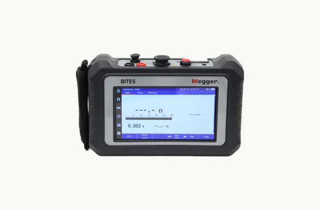
- Megger BITE5 — related equipment photograph only
- Power Device Analyzer / Curve Tracer | Keysight (technology background; not a supply claim)
- Keysight B1542A Pulsed IV Package User's Guide (technology background; not a supply claim)
- Semiconductor Teaching Labs | Keysight (technology background; not a supply claim)
- IT-3 Wafer-Level Electromigration for Reliability Monitoring: Quick-Turn Electromigration Stress with Correlation to Package-Level Stress (technology background; not a supply claim)
- PD1000A Power Device Measurement System for Advanced Modeling – Startup Guide (technology background; not a supply claim)
- DC-HTOL Burn-in Test System | Accel RF | Reliability Testing for Compound Semiconductors (technology background; not a supply claim)
- US20250076390A1 – Testing apparatus for power module with integrated dc test and withstand voltage test functions and test method using the same – Google Patents (technology background; not a supply claim)
- How to Perform VCSEL LIV Testing | Keysight (technology background; not a supply claim)
- US6911814B2 – Apparatus and method for electromechanical testing and validation of probe cards – Google Patents (technology background; not a supply claim)
The proposed configuration needs its own technical and acceptance evidence. Read the editorial policy.
Explore system selection guides ↗ · Browse advanced equipment families ↗
Explore the Wafer parametric electrical test system buying guide and RFQ checklist ↗
Continue the system review
Dimensional and surface metrology: Selection and Acceptance Guide
Dimensional and surface metrology: compare application boundaries, integration requirements, project cost and acceptance evidence for 8 equipment scopes.
8 equipment scopes · 9 min read · Related module image
Compare requirements and evidence ↗
Leak and functional performance testing: Selection and Acceptance Guide
Leak and functional performance testing: compare application boundaries, integration requirements, project cost and acceptance evidence for 9 equipment scopes.
9 equipment scopes · 10 min read · Related module image
Compare requirements and evidence ↗
Electronic assembly and battery testing: Selection and Acceptance Guide
Electronic assembly and battery testing: compare application boundaries, integration requirements, project cost and acceptance evidence for 8 equipment scopes.
8 equipment scopes · 10 min read · Related module image
Compare requirements and evidence ↗