
Industrial equipment. Informed decisions.8483454@gmail.com

IndustryApex · Engineering-led equipment supply

Crystal growth and wafer processing: Selection and Acceptance Guide

The decision in brief

For crystal growth and wafer processing selection, define incoming substrate state, required transformation and downstream handoff. Compare only equipment scopes that answer the same production or measurement question. Agree the required inputs, system interfaces and acceptance records before evaluating a configuration. This guide maps 26 related purchasing scopes to the evidence needed for a useful engineering proposal.

By IndustryApex Editorial · Reviewed 2026-10-23 · Editorial approach. Technical procurement guidance; the proposed equipment and commercial commitments require project-specific confirmation.
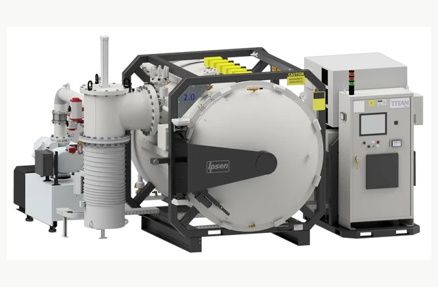
Ipsen TITAN vacuum furnace — related equipment reference; not the complete silicon carbide pvt crystal growth furnace
Ipsen TITAN vacuum furnace — related vacuum heat treatment furnace module/process reference; complete system not pictured. Related physical module or process reference; not the complete offered system or an IndustryApex installation.

What should you define before selecting the equipment?

Incoming substrate state, required transformation and downstream handoff. Write this decision into a revision-controlled requirement brief. Identify the product, material or test object, current conditions, required result and the information that is still unknown. Ask which question the proposed module actually answers before comparing quoted models.

Comparison error to avoid: treating separate wafer preparation steps as a complete device production line. The options below represent distinct purchasing boundaries. Some may operate together; their presence in this guide does not make them direct substitutes or a complete production line.

Compare the application and acceptance boundary

Use each entry to identify the relevant product guide and the first technical evidence to request. Keep the same drawing revision, feed condition or test object when comparing proposals for one scope.

Silicon carbide PVT crystal growth furnace: application fit and acceptance evidence

Grow a qualified silicon-carbide crystal using a physical-vapor-transport process.

PVT growth has distinct source, seed and thermal-field boundaries from silicon melt pulling.

What to specify
Source material, seed, boule objective, thermal design, vacuum and gas utilities.
What to verify in a representative trial
Verify representative crystal quality, process records, thermal stability and qualified material-yield evidence.

Review silicon carbide pvt crystal growth furnace configuration and OEM / ODM scope ↗

Request this equipment or OEM / ODM review ↗

Czochralski silicon crystal puller: application fit and acceptance evidence

Grow specified silicon crystals through a qualified melt-pulling process.

Czochralski growth requires melt and seed control and differs from float-zone purification and growth.

What to specify
Feedstock, crystal geometry, dopant objective, crucible, atmosphere and thermal requirements.
What to verify in a representative trial
Evaluate crystal dimensions, material analyses, defect evidence and repeatability under qualified trials.

Review czochralski silicon crystal puller configuration and OEM / ODM scope ↗

Request this equipment or OEM / ODM review ↗

Float zone silicon crystal growth system: application fit and acceptance evidence

Grow and refine suitable silicon rods using an engineered floating molten zone.

Float-zone processing avoids a conventional melt crucible and has different feed-rod and induction requirements from CZ.

What to specify
Feed-rod quality, crystal diameter, doping, induction design and atmosphere boundary.
What to verify in a representative trial
Verify representative crystal analyses, dimensional consistency and qualified zone-stability evidence.

Review float zone silicon crystal growth system configuration and OEM / ODM scope ↗

Request this equipment or OEM / ODM review ↗

Sapphire crystal growth furnace: application fit and acceptance evidence

Grow a specified sapphire crystal through an agreed qualified thermal route.

Sapphire growth requires material and thermal-field qualification rather than a generic heat-treatment furnace specification.

What to specify
Growth method, charge purity, crystal geometry, thermal design and atmosphere utilities.
What to verify in a representative trial
Assess representative crystal defects, usable geometry, material quality and repeat process records.

Review sapphire crystal growth furnace configuration and OEM / ODM scope ↗

Request this equipment or OEM / ODM review ↗

Gallium nitride MOCVD epitaxy reactor: application fit and acceptance evidence

Deposit qualified gallium-nitride epitaxial layers on specified semiconductor substrates.

MOCVD precursor delivery and epitaxy control differ from a generic protective coating process.

What to specify
Substrate, layer objectives, uniformity, precursor interfaces, abatement and analytical requirements.
What to verify in a representative trial
Verify representative layer analyses, wafer maps, contamination control and qualified process repeatability.

Review gallium nitride mocvd epitaxy reactor configuration and OEM / ODM scope ↗

Request this equipment or OEM / ODM review ↗

Molecular beam epitaxy system: application fit and acceptance evidence

Grow specified thin-film structures through an engineered molecular-beam epitaxy process.

MBE uses a distinct vacuum and source-control architecture from chemical-vapor epitaxy.

What to specify
Materials, substrate, source configuration, layer sequence, vacuum and in-situ diagnostics.
What to verify in a representative trial
Verify reference growth results, layer analyses, source stability and qualified contamination-control evidence.

Review molecular beam epitaxy system configuration and OEM / ODM scope ↗

Request this equipment or OEM / ODM review ↗

Chemical vapor deposition diamond reactor: application fit and acceptance evidence

Grow qualified diamond material using an engineered chemical-vapor deposition route.

Diamond growth requires application-specific plasma and substrate development and differs from generic PECVD film deposition.

What to specify
Substrate format, material objective, gas interfaces, thermal control and analytical acceptance.
What to verify in a representative trial
Evaluate representative diamond quality, thickness uniformity, defects and repeat qualified process results.

Review chemical vapor deposition diamond reactor configuration and OEM / ODM scope ↗

Request this equipment or OEM / ODM review ↗

Hydride vapor phase epitaxy reactor: application fit and acceptance evidence

Grow specified compound-semiconductor layers through a qualified hydride-vapor-phase process.

HVPE has distinct chemistry and reactor interfaces from MOCVD and requires specialist process development.

What to specify
Material system, substrate, growth objective, gas compatibility, abatement and metrology.
What to verify in a representative trial
Verify representative layer structure, purity, uniformity and qualified reactor-control records.

Review hydride vapor phase epitaxy reactor configuration and OEM / ODM scope ↗

Request this equipment or OEM / ODM review ↗

Wafer chemical mechanical polishing system: application fit and acceptance evidence

Planarize specified wafer materials using a qualified combined chemical and mechanical process.

CMP depends on slurry, pad and material-stack interactions and differs from ordinary mechanical lapping.

What to specify
Wafer size, film stack, removal target, defect limits, slurry and cleaning interfaces.
What to verify in a representative trial
Compare wafer maps, removal consistency, surface defects and reference-metrology correlation.

Review wafer chemical mechanical polishing system configuration and OEM / ODM scope ↗

Request this equipment or OEM / ODM review ↗

Wafer back grinding and thinning system: application fit and acceptance evidence

Thin suitable wafers through an engineered supported grinding and stress-management workflow.

Wafer thinning includes handling and damage control distinct from generic surface grinding of metal parts.

What to specify
Wafer material, final thickness, temporary support, device features and downstream singulation.
What to verify in a representative trial
Verify thickness maps, warpage, damage evidence and handling yield on representative wafers.

Review wafer back grinding and thinning system configuration and OEM / ODM scope ↗

Request this equipment or OEM / ODM review ↗

Stealth laser wafer dicing system: application fit and acceptance evidence

Singulate qualified wafers using an engineered internal laser-modification and separation process.

Stealth dicing differs from surface laser ablation and requires material-specific optical feasibility.

What to specify
Wafer transparency, device layout, thickness, street geometry, tape and separation method.
What to verify in a representative trial
Verify singulation quality, edge damage, alignment and representative die-strength evidence.

Review stealth laser wafer dicing system configuration and OEM / ODM scope ↗

Request this equipment or OEM / ODM review ↗

Precision wafer bonding system: application fit and acceptance evidence

Join specified wafer structures with qualified alignment and bonding conditions.

Wafer bonding requires surface preparation and process qualification and differs from general adhesive assembly.

What to specify
Wafer materials, size, bond method, alignment, surface condition and contamination limits.
What to verify in a representative trial
Verify alignment, void maps, bond integrity and representative wafer-level metrology.

Review precision wafer bonding system configuration and OEM / ODM scope ↗

Request this equipment or OEM / ODM review ↗

Wafer laser annealing system: application fit and acceptance evidence

Apply a qualified localized thermal treatment to specified semiconductor structures.

Laser annealing has distinct optical absorption and thermal-budget requirements from furnace annealing.

What to specify
Wafer stack, treatment objective, optical response, thermal budget and process uniformity.
What to verify in a representative trial
Verify representative material or electrical results, thermal consistency and defect measurements.

Review wafer laser annealing system configuration and OEM / ODM scope ↗

Request this equipment or OEM / ODM review ↗

Semiconductor ion implantation system: application fit and acceptance evidence

Introduce specified dopant species into suitable substrates through a qualified ion-beam process.

Implantation requires beam, dose and contamination controls and differs from diffusion furnace treatment.

What to specify
Substrate, dopant, dose and energy objectives, throughput, handling and abatement interfaces.
What to verify in a representative trial
Verify dose and beam uniformity, contamination controls and qualified material-analysis results.

Review semiconductor ion implantation system configuration and OEM / ODM scope ↗

Request this equipment or OEM / ODM review ↗

ICP reactive ion etching system: application fit and acceptance evidence

Pattern specified materials through an engineered inductively coupled plasma etch process.

ICP etching depends on chemistry, selectivity and substrate control and differs from physical sputter removal.

What to specify
Material stack, mask, profile target, selectivity, substrate cooling and exhaust treatment.
What to verify in a representative trial
Verify etch profiles, uniformity, residues and representative mask or substrate effects.

Review icp reactive ion etching system configuration and OEM / ODM scope ↗

Request this equipment or OEM / ODM review ↗

Deep reactive ion etching system: application fit and acceptance evidence

Form qualified deep structures in suitable substrates through an engineered plasma etch sequence.

DRIE requires sidewall and aspect-ratio qualification beyond a shallow etch rate specification.

What to specify
Substrate, mask, feature geometry, depth, sidewall targets and thermal control.
What to verify in a representative trial
Inspect representative profiles, depth maps, roughness and process repeatability.

Review deep reactive ion etching system configuration and OEM / ODM scope ↗

Request this equipment or OEM / ODM review ↗

Semiconductor wet process bench: application fit and acceptance evidence

Clean or etch specified semiconductor materials in a qualified chemical-processing installation.

A wet bench requires contamination, chemistry and substrate handling controls distinct from a general parts washer.

What to specify
Substrates, chemistry compatibility, bath sequence, particle limits, handling and exhaust interfaces.
What to verify in a representative trial
Verify cleaning or etch results, carryover, contamination and qualified chemical-delivery controls.

Review semiconductor wet process bench configuration and OEM / ODM scope ↗

Request this equipment or OEM / ODM review ↗

Vapor phase MEMS release etching system: application fit and acceptance evidence

Release specified microstructures through a qualified vapor-phase sacrificial-material removal process.

Vapor release differs from liquid etching and needs selectivity and materials-compatibility evidence.

What to specify
Device stack, sacrificial material, structural materials, release geometry and exhaust treatment.
What to verify in a representative trial
Verify representative release completion, stiction behavior, residues and protected-material integrity.

Review vapor phase mems release etching system configuration and OEM / ODM scope ↗

Request this equipment or OEM / ODM review ↗

Rapid thermal processing system: application fit and acceptance evidence

Apply a qualified short-duration thermal cycle to specified wafers.

RTP thermal uniformity and emissivity effects differ from a long furnace soak.

What to specify
Wafer materials, thermal budget, atmosphere, temperature measurement and device-stack requirements.
What to verify in a representative trial
Verify reference thermal behavior, wafer uniformity and representative material or electrical results.

Review rapid thermal processing system configuration and OEM / ODM scope ↗

Request this equipment or OEM / ODM review ↗

Semiconductor diffusion oxidation furnace: application fit and acceptance evidence

Process specified wafers through a qualified thermal oxidation or diffusion sequence.

Semiconductor furnace purity and wafer-loading boundaries differ from metal heat treatment.

What to specify
Wafer size, process atmosphere, layer or dopant objective, contamination limits and batch format.
What to verify in a representative trial
Verify wafer maps, reference analyses, contamination and repeat batch results.

Review semiconductor diffusion oxidation furnace configuration and OEM / ODM scope ↗

Request this equipment or OEM / ODM review ↗

Electron beam lithography system: application fit and acceptance evidence

Write specified resist patterns using an engineered electron-beam lithography workflow.

Electron-beam patterning requires resist and proximity-effect qualification and differs from optical mask exposure.

What to specify
Pattern dimensions, substrate, resist, alignment, write field and charging behavior.
What to verify in a representative trial
Verify reference patterns, placement, critical dimensions and representative process repeatability.

Review electron beam lithography system configuration and OEM / ODM scope ↗

Request this equipment or OEM / ODM review ↗

UV mask alignment lithography system: application fit and acceptance evidence

Align and expose specified resist-coated substrates through a qualified optical mask process.

Mask alignment and exposure uniformity differ from a laser-direct-writing workflow.

What to specify
Substrate, mask, resist, alignment accuracy, exposure mode and required feature geometry.
What to verify in a representative trial
Verify overlay, exposure uniformity, pattern dimensions and repeated substrate handling.

Review uv mask alignment lithography system configuration and OEM / ODM scope ↗

Request this equipment or OEM / ODM review ↗

Nanoimprint lithography system: application fit and acceptance evidence

Replicate specified micro- or nanoscale patterns through a qualified imprint process.

Imprinting requires mold, release and resist qualification and differs from ordinary embossing of packaging film.

What to specify
Template, substrate, resist, feature dimensions, residual layer and defect criteria.
What to verify in a representative trial
Inspect pattern transfer, alignment, release defects and representative mold-cycle behavior.

Review nanoimprint lithography system configuration and OEM / ODM scope ↗

Request this equipment or OEM / ODM review ↗

PCB laser direct imaging system: application fit and acceptance evidence

Image specified PCB resist patterns using a qualified direct optical exposure process.

LDI is a photolithographic workflow and differs from marking or ablating a finished board.

What to specify
Panel dimensions, resist response, feature geometry, registration and handling requirements.
What to verify in a representative trial
Verify line and space patterns, registration, exposure consistency and representative panel results.

Review pcb laser direct imaging system configuration and OEM / ODM scope ↗

Request this equipment or OEM / ODM review ↗

Wafer resist coat and develop track: application fit and acceptance evidence

Prepare and develop specified wafer resists through an engineered coating and processing sequence.

Resist processing has film and contamination duties separate from the exposure tool.

What to specify
Wafer format, resist chemistry, film target, baking, developing and transfer interfaces.
What to verify in a representative trial
Verify coating maps, edge behavior, developed patterns and contamination or repeatability evidence.

Review wafer resist coat and develop track configuration and OEM / ODM scope ↗

Request this equipment or OEM / ODM review ↗

Plasma photoresist stripping system: application fit and acceptance evidence

Remove qualified resist or organic residues from specified substrates using a controlled plasma process.

Plasma stripping requires substrate and residue selectivity and differs from etching the underlying functional layer.

What to specify
Resist, substrate stack, residue, thermal limits, endpoint method and exhaust requirements.
What to verify in a representative trial
Verify removal, substrate integrity, contamination and repeat processing on representative structures.

Review plasma photoresist stripping system configuration and OEM / ODM scope ↗

Request this equipment or OEM / ODM review ↗

Crystal growth and wafer processing integration requirements

Connect the incoming material state to the required feature, surface or material-property result. State preparation, fixtures, process services, downstream steps and the inspection method. Qualify representative parts or specimens before accepting a production-envelope claim. A single process module does not establish the capability of the complete manufacturing route.

Interface Information to record Approval needed
Incoming material or test object Drawing or composition revision, normal variation, presentation and preparation. Process or quality owner confirms the representative case.
Utilities and controls Actual conditions, connection points, available signals, permissions and data format. Site engineering confirms the connection boundary.
Outgoing product and residuals Accepted output, rejects, residual streams and downstream handoff. The receiving operation confirms its requirements.
Trials and records Method, samples, reference conditions, responsible party and acceptance decision. The designated technical owner approves the test plan.

Crystal growth and wafer processing project cost: what belongs in the scope?

Check the quotation boundary for clean utilities, handling, consumables and downstream qualification. Include tooling, material preparation, utilities, consumables, handling, downstream finishing and inspection. Identify which process-development or qualification tasks are included and who owns the resulting records.

Compare complete scopes using your measured inputs and written quotations. Record production calendar, utility assumptions, consumable replacement basis and the cost of rejected output where relevant. Mark unknown values for confirmation. Request the exclusions and optional items in writing; a generic catalogue price or assumed payback is not a project estimate.

Use the procurement cost tools to organize explicit assumptions, then reconcile them with the proposal.

Crystal growth and wafer processing acceptance criteria and trial records

The evidence plan should establish representative substrates, agreed property measurements and traceable process records. Use the product-specific trial questions above to define the actual method. Agree specimen or feed selection, operating cases, test duration where relevant, records, acceptance authority and the handling of a failed result before ordering.

Separate factory acceptance from checks that depend on the installed site. Identify the witnesses, instruments or analytical methods, traceability records and retest responsibility. Preserve the requirement revision, test conditions and exceptions with the result. A witnessed demonstration supports only the tested scope and conditions; record any untested materials, variants or operating states.

Crystal growth and wafer processing OEM / ODM project brief

IndustryApex engineers review the application and develop the equipment and supply scope for your project. For OEM / ODM, distinguish branding and documentation requirements from functional, layout, tooling, control or process changes.

  • Relevant product family and the required production or measurement result.
  • Product-specific technical inputs identified in the comparison above.
  • Existing equipment, utilities, controls and upstream or downstream interfaces.
  • Destination country and city, installation scope and purchasing window.
  • Representative trial material and the required acceptance records.
  • OEM branding or requested ODM changes, with the constraints and approval owner.

Supply availability, exact configuration, customization feasibility, installation and support responsibilities are confirmed in the individual proposal.

Request an engineering and OEM / ODM review ↗

Buyer questions

How should I start crystal growth and wafer processing selection?

Define incoming substrate state, required transformation and downstream handoff. Identify the relevant purchasing boundary in the comparison, then prepare its specific inputs and representative trial evidence before selecting a model.

Which acceptance evidence belongs in this crystal growth and wafer processing RFQ?

Agree representative substrates, agreed property measurements and traceable process records. Add the product-specific trial points in this guide, a controlled method, responsible technical owner and a documented disposition for failed or untested cases.

What should the project cost comparison include?

Include clean utilities, handling, consumables and downstream qualification. Compare written equipment and service scopes using the actual operating profile, explicit assumptions and confirmed exclusions. A project estimate requires a configuration and site review.

Can IndustryApex review OEM / ODM requirements?

Yes. Send the required result, relevant product family, interfaces, destination and requested branding or functional changes. IndustryApex engineers assess the configuration and equipment supply scope. Feasibility, quotation, installation and support commitments are confirmed for that project.

Technical reference basis

The selection and evidence questions draw on the product library’s technical background records. References may describe original research, a process method or a related physical module. They do not establish an offered configuration, supply relationship or commercial readiness.

  • PVA TePla crystal-growth technology portfolio (technology background; not a supply claim)
  • Ipsen TITAN vacuum furnace — related equipment photograph only
  • PVA TePla Czochralski crystal growth (technology background; not a supply claim)
  • Inductotherm Heavy steel shell furnace — related equipment photograph only
  • A Pioneering Legacy in Furnaces for Sapphire Crystal Growth (technology background; not a supply claim)
  • AIXTRON MOCVD technology (technology background; not a supply claim)
  • Th (technology background; not a supply claim)
  • Busch R5 RA 0155 A — related equipment photograph only
  • On the optimization of a dc arcjet diamond chemical vapor deposition reactor (technology background; not a supply claim)
  • WO2020252481A1 – Hydride vapor phase epitaxy reactors – Google Patents (technology background; not a supply claim)
  • Chemical-mechanical polishing (CMP) (technology background; not a supply claim)
  • Lapmaster Wolters Model 36 open-face flat lapping machine — related equipment photograph only
  • DISCO wafer grinding and stealth-dicing process scope (technology background; not a supply claim)
  • Kent USA KGS-2460AHD — related equipment photograph only
  • Telesis ProStation marking workstation/enclosure (laser configuration varies) — related equipment photograph only
  • EV Group lithography bonding and resist-processing portfolio (technology background; not a supply claim)
  • Kistler NC joining system — related equipment photograph only
  • Fully Automated Wafer Laser Annealing Machine | HGLaser (technology background; not a supply claim)
  • Axcelis | Ion Implantation | Purion Ion Implanters (technology background; not a supply claim)
  • ICP Etching – Oxford Instruments (technology background; not a supply claim)
  • SPT plasma etching technologies (technology background; not a supply claim)
  • Semiconductor Wet Bench Equipment (technology background; not a supply claim)
  • Ecoclean EcoCcube — related equipment photograph only
  • HF Vapor Phase Etcher – Idonus VPE 100 – PoliFab – Politecnico di Milano (technology background; not a supply claim)
  • Company Introduction and Main Products (technology background; not a supply claim)
  • Diffusion/Oxidation Furnace – Semiconductor Device Fabrication Lab (technology background; not a supply claim)
  • Ipsen ATLAS atmosphere furnace — related equipment photograph only
  • Electron Beam Lithography System – 100 KeV – The Advanced Science Research Center (technology background; not a supply claim)
  • Banner Engineering VE smart camera — related equipment photograph only
  • EV Group nanoimprint lithography (technology background; not a supply claim)
  • LDI-V series LDI Laser Direct Imager (technology background; not a supply claim)
  • DOPAG Multifunctional robot-assisted adhesive dispensing cell — related equipment photograph only
  • Plasma Photoresist Stripping Platform | NineScrolls LLC (technology background; not a supply claim)

The proposed configuration needs its own technical and acceptance evidence. Read the editorial policy.

Explore system selection guides ↗ · Browse advanced equipment families ↗

Continue the system review

WhatsApp